The Semiconductor Chip Manufacturing Process
If you wish to compose an e-mail, index a database of web pages, stream a kitten video in 720p or render an explosion at 60 frames per second, you must first build a computer.
And to build a computer, you must first design and fabricate the tiny processors (semiconductor chips) that rapidly churn through the millions of discrete computational steps behind every one of those digital actions, taking a new step approximately 3 billion times per second.
To do all this, you are probably going to need chip-manufacturing machines/quality control/surface analysis machines from companies such as Applied Materials, ASML, Hitachi High tech, JEOL, SPECS, some of the suppliers of such equipment to the semiconductor industry.
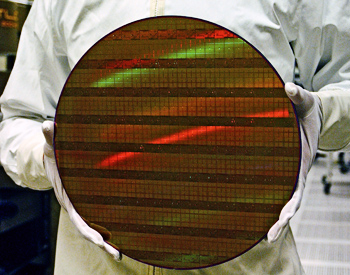
Applied's machines subject silicon wafers (such as the Intel wafer shown below) to incredibly intense vacuums, caustic chemical baths, high-energy plasmas, intense ultraviolet light, Hydrofluoric acid etching baths, and more, taking the wafers through the hundreds of discrete manufacturing steps required to turn them into CPUs, memory chips and graphics processors.

Because those processes aren't exactly friendly to humans, much of this work happens inside sealed chambers where robot arms move the wafers from one processing station to another. The machines themselves are housed within clean rooms whose scrubbed air (and bunny-suited employees) keep the risk of aerial contamination low: A single dust particle from your hair is all it takes to ruin a CPU that might sell for $500, so companies are eager to minimize how often that happens.
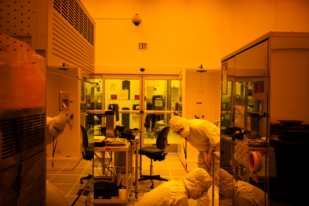
Wired/com recently toured Applied Materials' Maydan Technology Center, a state-of-the-art clean room in Santa Clara, California, where Applied develops and tests its machines.
Its 39,000 square feet of ultraclean workspace equals about 81 yards of a football field, and is divided into three huge "ballrooms," each of which is crammed full of Applied's multimillion-dollar machines, alongside pipes, tubes, spare parts, tanks of caustic chemicals, Craftsman tool chests and huge racks of silicon wafers. To get inside, you must suit up in a bunny suit, with a face mask and goggles, two pairs of gloves, and shoe-covering footies. We couldn't even take a reporter's notebook inside: Instead, Applied's staff gave us a shrink-wrapped, specially sanitized clean-room notebook and clean-room pen to use.
It's not a manufacturing facility. Instead, this clean room simulates the fabs where Applied's machines will be used, enabling the company (and its customers) to test out new techniques and processes before putting them on the production line. As such, it provides a rare glimpse inside the world of cutting-edge semiconductor manufacturing.
Top photo: Jon Snyder/Wired.com
Bottom photo: Intel
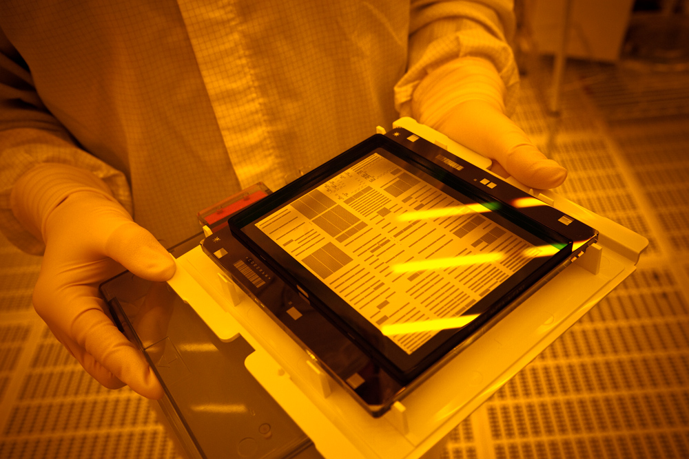
Photomask
The heart of chip manufacturing is lithography. It's like silkscreening, except instead of squeegeeing ink through a silk template onto a cotton T-shirt, you're shining ultraviolet light through a glass photomask onto a silicon substrate coated with an organic compound called photoresist.
Where the UV light shines through, it chemically weakens the photoresist, leaving a pattern on the surface of the silicon. Then the wafer is sent through a chemical bath that etches trenches into the exposed substrate, while leaving the areas covered by the photoresist untouched.
After removing the photoresist, other machines can fill those trenches with various materials, such as copper or aluminum, that comprise the components of the processor. A process called Chemical Vapor Deposition is used to deposit various materials.
Shown here is a photomask, which bears the patterns that will be printed onto a wafer.
Photo: Jon Snyder/Wired.com
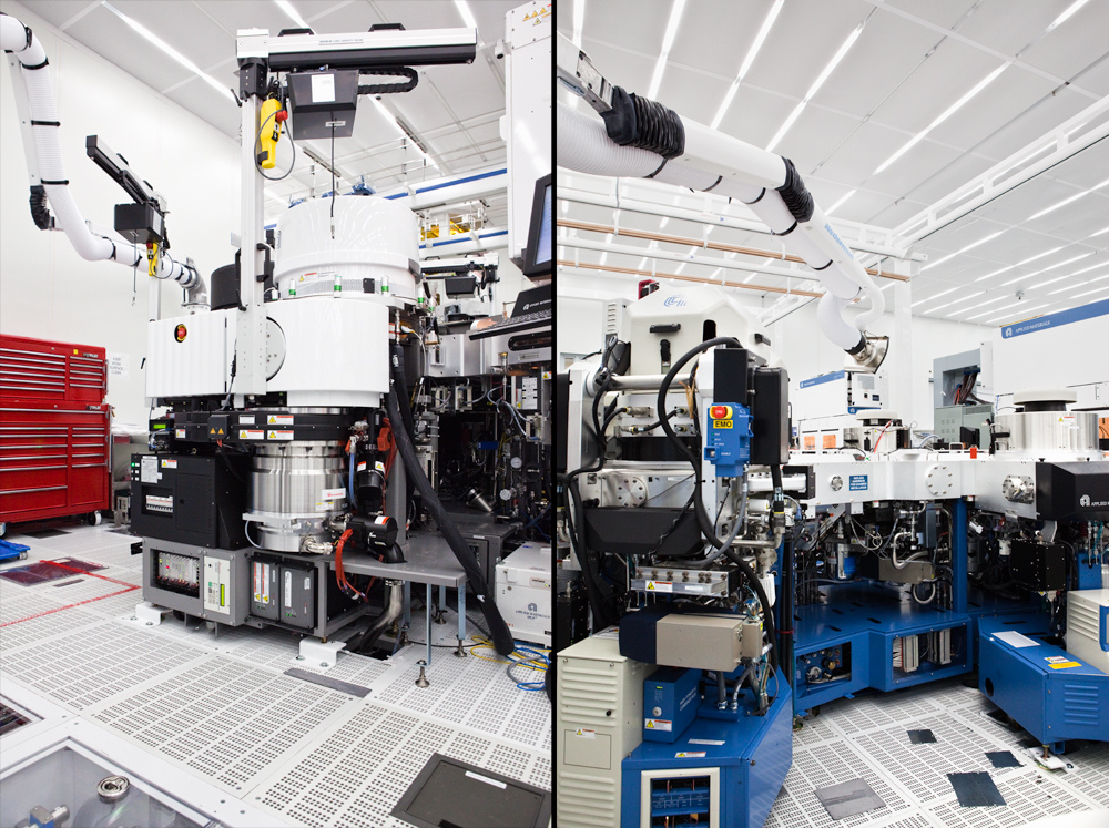
Deposit, Etch, Repeat
As a wafer is sent through the manufacturing facility, it can go through as many as 250 different steps. These processes include depositing films of various materials, then etching them to form transistors and copper wiring.
On the right is one of Applied Materials' Endura machines. The Endura platform is a modular, configurable system used to deposit metals and metal alloys on the wafer. It has been used in the manufacturing of almost every chip made in the past 20 years, according to Applied.
On the left is an Applied Tetra III advanced reticle-etch system. This system is used by virtually every maskmaker in the world for the development and production of 45-nanometer masks.
Because it's developing and testing new manufacturing equipment, a huge amount of Applied's expenditures go towards research. In 2009, the company spent $934 million, or about 20 percent of its revenue, on R&D.
Photo: Jon Snyder/Wired.com
The current state of the art for chip manufacturing is 30 nanometers, which means the average size of a chip component is just 30 billionths of a meter across.
Chip manufacturers are currently working on 22-nanometer designs, which are even smaller.
Adding to the challenge is the fact that some of these features are far deeper than they are wide -- in some cases, by a factor of 60 to 1. That means the etching systems have to be capable of creating extremely deep and narrow trenches in silicon, at the nanometer scale, with immense precision.
The lithography room is lit with yellow light to avoid interference with the UV light used with the photomasks.
Photo: Jon Snyder/Wired.com
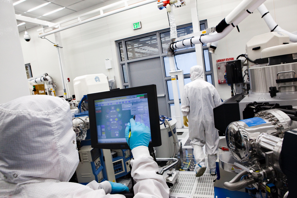
Extreme Vacuum
A technician works on the touchscreen interface of an Endura system.
On the right is one of the large silver pumps used to create extreme vacuums inside the machine -- as low as 10-12 atmospheres. (By comparison, the air pressure at 200 kilometers [about 124 miles] above the Earth, where the Space Shuttle orbits, is about a hundred times thicker, at about 10-10 atmospheres.)
Photo: Jon Snyder/Wired.com
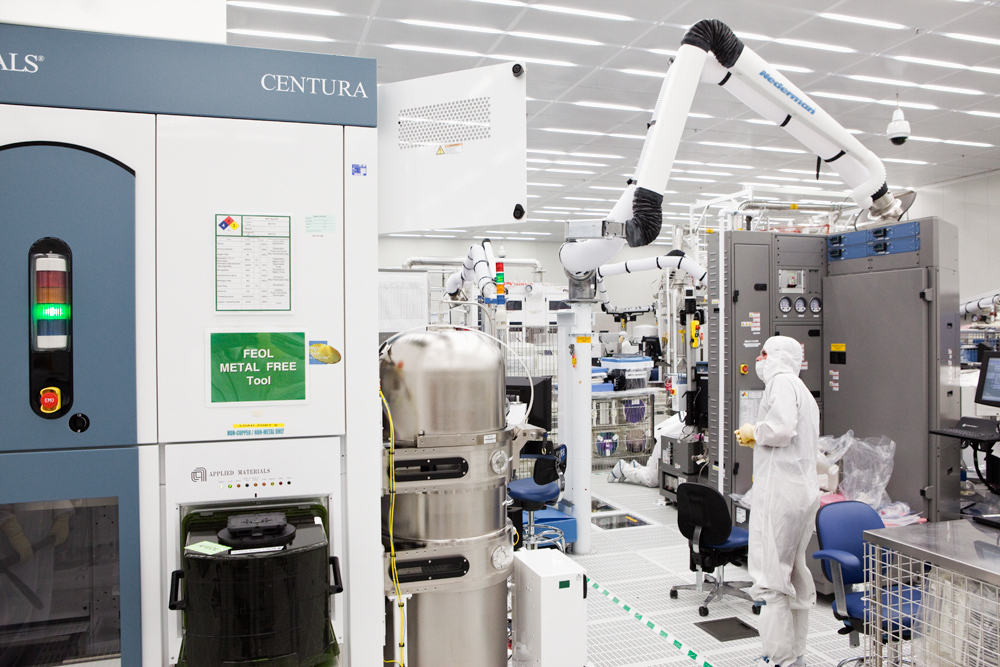
No Metal Here
The silver metal device on the right side of this Centura machine is a batch loader, used to quickly depressurize a stack of wafers prior to feeding them into the machine for processing.
The green "metal free tool" sign indicates that this machine is used in a part of the process prior to the addition of copper circuits. Copper is a contaminant that can mess up nonmetallic stages of the manufacturing process, so the machines that add copper need to be carefully segregated.
Photo: Jon Snyder/Wired.com

FOUP
Over the past several decades, the wafers upon which chips are made have steadily increased in size, enabling manufacturers to cram more chips on each disk. Since 2000, the industry standard has been 300 mm [about a foot in diameter].
To simplify transportation and minimize the risk of contamination, fabs make use of "front-opening unified pods," or FOUPs. Each one holds 25 wafers in a sterile, clean environment.
FOUPs can be docked onto the front of most of Applied's machines. The machines then suck the wafers inside and automatically process them one-by-one in quick succession.
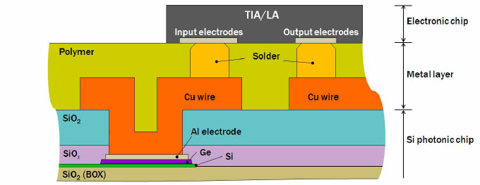
This above is a schematic cross section of a silicon chip for a transimpedance amplifier/limiting amplifier (TIA/LA) circuit. This schematic appeared in the following article:
Monolithic integration of a silica AWG and Ge photodiodes on Si photonic platform for one-chip WDM receiver from Optics Express 20(8):9312-21 · April 2012
BOX stands for Burried Oxide. WDM is wavelength-division multiplexing a technology which multiplexes a number of optical carrier signals onto a single optical fiber by using different wavelengths (i.e., colors) of laser light. AWG means arrayed-waveguide grating. These devices are capable of multiplexing a large number of wavelengths into a single optical fiber, thereby increasing the transmission capacity of optical networks considerably.
The SiO2 layer in the top chip is produced by oxidizing the Silicon wafer in a solution of Hydrogen Peroxide. if you want to etch the SiO2, Hydro Fluoric acid is used. In graduate school I did experiments like these. Copper is deposited using a technique called sputtering.
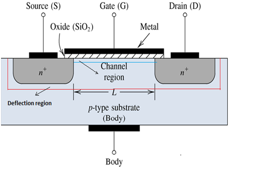
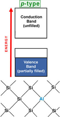
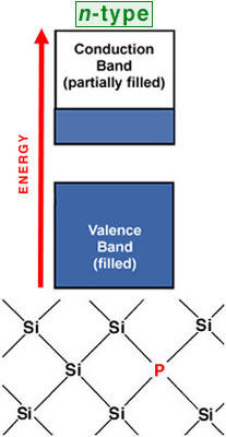
And this above is a schematic of a MOSFET, a Metal Oxide Field Effect Transistor. The n and p type layers refer to Silicon that has been doped with positive or negative dopants, elements such as Phosphorus and Aluminum (see image below).
 |
 |
|---|
Doping means the introduction of impurities into the semiconductor crystal to deliberately change its conductivity due to deficiency or excess of electrons. Normally Trivalent and Pentavalent elements are used to dope Silicon and Germanium. When an intrinsic semiconductor is doped with Trivalent impurity it becomes a P-Type semiconductor. Doping is done in semiconductors in order to increase their conductivity, as normally they have very little conductivity because the band gap between valence and conduction band is large. Extrinsic semiconductors are formed as a result of doping. Diffusion is a technique used in doping. Simply put, the doping element diffuses into the crystal lattice of the Silicon wafer. Another technique used is Ion Implantation. See the article references below from Halbleiter for more interesting details.
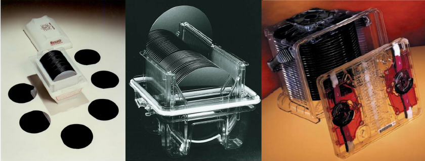
The silicon chip always starts with a Silicon wafer. Below is a photo of silicon wafers in special polycarbonate transparent packaging. These are 200 mm wafers. The current state of the art fabs use 300 mm wafers.
In semiconductor device fabrication, the various processing steps fall into four general categories: deposition, removal, patterning, and modification of electrical properties.
Deposition is any process that grows, coats, or otherwise transfers a material onto the wafer. Available technologies include physical vapor deposition (PVD), chemical vapor deposition (CVD), electrochemical deposition (ECD), molecular beam epitaxy (MBE) and more recently, atomic layer deposition (ALD) among others.
Removal is any process that removes material from the wafer; examples include etch processes (either wet or dry) and chemical-mechanical planarization aka polishing (CMP).
Patterning is the shaping or altering of deposited materials, and is generally referred to as lithography. For example, in conventional lithography, the wafer is coated with a chemical called a photoresist; then, a machine called a stepper focuses, aligns, and moves a mask, exposing select portions of the wafer below to short wavelength light; the exposed regions are washed away by a developer solution. After etching or other processing, the remaining photoresist is removed by plasma ashing.
Modification of electrical properties has historically entailed doping transistor sources and drains (originally by diffusion furnaces and later by ion implantation). These doping processes are followed by furnace annealing or, in advanced devices, by rapid thermal annealing (RTA); annealing serves to activate the implanted dopants.
Modification of electrical properties now also extends to the reduction of a material's dielectric constant in low-k insulators via exposure to ultraviolet light in UV processing (UVP).
Modern chips have up to eleven metal levels produced in over 300 sequenced processing steps.
Last updated 27.9.2017
by Rami E. Kremesti M.Sc., CWEM, CSci, CEnv
References:
1. A Chip Is Born: Inside a State-of-the-Art Clean Room - by Jon Snyder Gear, Wired Magazine , Date of Publication: 10.19.10.
2. Monolithic integration of a silica AWG and Ge photodiodes on Si photonic platform for one-chip WDM receiver from Optics Express 20(8):9312-21 · April 2012
3. Silicon Crystal Growth and Wafer Technologies, Proceedings of the IEEE 100(Special Centennial Issue):1454-1474 · May 2012
4. Semiconductor Technoilogy from A to Z : https://www.halbleiter.org/en/waferfabrication/doping/