![]()
Semiconductor Ultra Pure Water Treatment
Introduction
Water for Semiconductor Industry – Semiconductor water treatment is Ultra-Pure Water treatment aiming to reduce in-organics, organics, particulates (inorganic, organic and biological) and gases in water to the ppb range.
The most widely used requirements for UPW quality are documented by ASTM D5127 “Standard Guide for Ultra-Pure Water Used in the Electronics and Semiconductor Industries”.
The technologies used are UF, RO, EDI, Mixed Bed Ion Exchange, Advanced Oxidation Processes (AOP’s), UV, Active Carbon Filtration, combustion/heat and sometimes Membrane Contactors for degasification. All piping used must be semiconductor grade to prevent particle and fibre shedding and leaching of any chemicals. RO membranes need to be semiconductor grade same as any ion exchange resins.
Chemicals Used
Chemicals used have to be semiconductor grade. Some semiconductor grade ion exchange resins are sometimes used. UPW tanks are usually blanketed with Nitrogen to prevent the dissolution of gases such as O2 and CO2.
Production and Assembly Facilities
Production facilities in the semiconductor industry are Clean Room type with HEPA fitted HVAC systems that filter out dust from the air. There are several classes of clean rooms depending on the size and number of dust particles per m3 of air. Workers in a semiconductor fab are normally fitted with “bunny suits” to prevent particle, bacteria and hair shedding from the body.
Impurities in semiconductor processing water have a negative impact on production yields due to defects caused by impurities in the production and lithographic process. Pumps used in conveying ultra pure semiconductor grade water have to be of special design to minimise particle shedding.

Semiconductor Grade Water Treatment Process Schematic
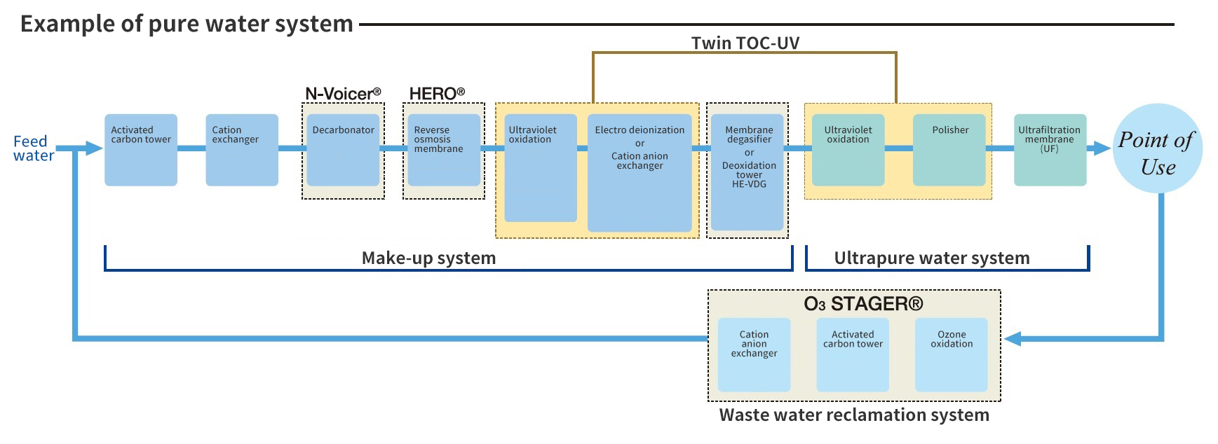
Nomura Japan Ultra Pure Water Treatment Process
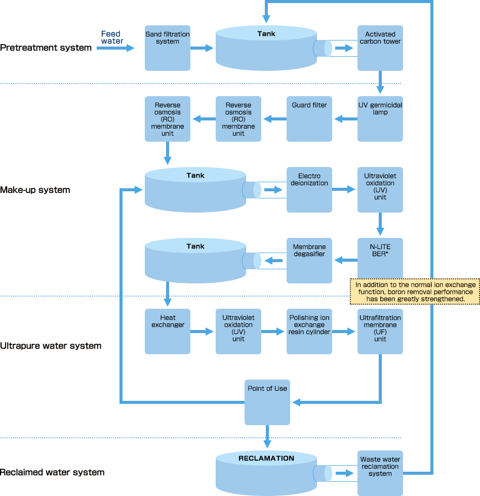
Ultra Pure Water Treatment System Without Chemicals for Regeneration of Resins
Monitoring Semiconductor Water Quality
Monitoring the impurities in semiconductor fab water requires specialised analytical instruments. From sampling and measuring to characterisation and more, Air Liquide’s world-class analytical services are key in helping electronics manufacturers control, monitor and improve their Fab throughput, and assure the quality of electronics devices.
TOC analysers, conductivity and particle counters are among the instruments used. I personally used to look at Silicon chips under the AFM microscope when I did my M.Sc research to identify contaminants.
Several parameters are monitored for quality control of semiconductor UPW. These parameters, their points of measurement and measurement method are identified in Table 1. A brief discussion of the main kinds of contaminants, methods of control of their level in UPW, and their typical specified limits is provided below.
Parameter Measured – (POD/POC) – Test Method
TOC – Online – Conductivity/CO2
Organic Ions – Lab – Ion Chromatography
Other Organics – Lab – LC-MS, GC-MS, LC-OCD
Total Silica – Lab – ICP-MS or GFAAS
Particle Monitoring – Online – Light Scatter
Particle Count – Lab SEM – capture filter at various pore sizes
Cations, Anions, Metals – Lab – Ion Chromatography, ICP-MS
Dissolved O2 – Online – Electric Cell
Dissolved N2 – Online – Electric Cell
Legend:
ICP-MS – inductively coupled plasma – mass spectrometry
LC – liquid chromatography
GC – gas chromatography
MS – mass spectrometry
SEM – scanning electron microscopy
GFAAS – graphite furnace atomic absorption spectroscopy
LC-OCD – liquid chromatography – organic carbon detection
POD/POC = Point of Delivery or Point of Connection
Articles
Here is an interesting article from Wired Magazine about how “A Chip is Born“. I adapted this article to describe the semiconductor manufacturing process.
Here is an interesting article from Hager El Sasser on this subject.
Waste Water
Waste water from the rinsing operations are normally high in some heavy metals like Copper and could contain toxic ions such as Fluoride. Clarifiers/Precipitation are one technology used for purification of this waste water as well as selective Ion Exchange and RO membranes. It is possible to recycle this water internally as it is still quite clean water.
Here are some topics on Semiconductor Waste Water Treatment:
Hydrofluoric (HF) Acid Waste Water System
Heavy Metal Waste Treatment System
Cyanide Treatment System
Ammonium/Ammonia Treatment System
Backgrind Waste Treatment System
Diluted Palladium Waste Recovery System
Aurum (Gold) Waste Recovery System
Copper Waste Treatment System
Suppliers
Major suppliers of water treatment plants for the Semiconductor industry are:
GE Water aquired by SUEZ in 2017
Veolia
Siemens Water now Evoqua, acquired by Xylem
OVIVO
Bosch
DOW has Special Semiconductor Grade RO membranes.
Nomura Japan
Organo Japan
Conclusion
Since I got my M.Sc. in Industrial Chemistry in 1998, I have been fascinated by semiconductors and ultra pure water treatment. I hope you have found this page useful. Semiconductor grade water is on a completely different level of purity.
References
International Technology Roadmap for Semiconductors: https://www.itrs2.org/
https://www.nomura-nms.co.jp/english/product/02_01_02.html
Compiled by Rami E. Kremesti M.Sc. , CSci, CWEM, CEnv
Last updated November 28, 2025
Contact us for more information on Water for Semiconductor Industry.
If you found this page useful, please leave us a positive review on Google.
About the Author:
Rami Elias Kremesti is a chartered water and waste water treatment specialist based out of the UK. He holds an M.Sc. degree in industrial chemistry from the USA. He is the MD of Kremesti Environmental Consutling Ltd.

Rami Elias Kremesti Portrait